
How is LED produced?
 How LED is working ?
LED (Light-Emitting Diode) technology is based on effect of electroluminescence with structure of two semiconducting materials combined together.
White, green and blue leds are based on a special semiconductor type - InGaN (indium gallium nitride).
Semiconductor region P contains positively while N type negatively charged carriers. These two materials together create every diode. Once the voltage is applied between electrodes the current starts to flow. Basically electrons move in one direction while holes travel in the opposite direction. Free electrons fill holes when approaching to it. Hole exists on lower energy levels then electrons, so the energy must be emitted to equalize.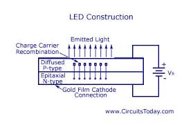
When electron looses its energy, the energy is released in a form of a photon – the basic smallest amount of the light emitted.
The amount of energy of photons is reflected in frequency (1/ L – reversal of wave length) and the color of the light. Colour and efficiency of light output depends on material preparation and P and N semiconductor type used.
By injecting impurities into materials, manufacturers of crystals influence several characteristics of future LED product.
Drawing belongs to website : www.circuitstoday.com
Specialized OEMs produce crystals (called also chips or dies, main components – hearts of LED) which are further used by LED manufacturers.
There are only a few real LED chips manufactures thus the rest must buy chips for their production. Value (cost) is related to size and quality of crystal strongly influencing the price of final LED. Quality, lighting performance and life depends fundamentally on the chip which is grown in epi (epitaxial) growth process.
These days sapphire substrates are the most common materials in producing chip wafers - thin slice of semiconducting material used in LED production. Semiconductor wafers are generally round and made with different diameters, usually from 50mm up to 200mm.
Not all surface of the wafer contains the same quality of chips, the best quality of crystal is in the middle part of the disc and it decreases with its radius so the edge of the wafer disc can not be used at all.
Wafers surface is cut and divided into a number of a small led dies. For example small 2’’(50mm) disc contains aprox 63 000 pcs of 45x45mil Led chips, while 200mm one contain 111 000 pcs.
The process of manufacturing crystals differentiates manufacturers, because usually wafer house is not final LED manufacturer.
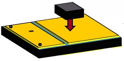
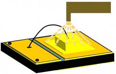
Process of LED assembly starts, from attaching a die to package substrate.
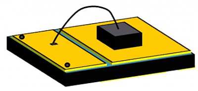
Then another side of the chip is connected to external electrode ( pad) with golden wire.
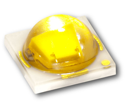
Third part is to cover the die with phosphor and encapsulation process, closing all with lens doom to direct the light and protect the structure.
In the meantime, in the production process, there are several pitstops for testing, mainly done at the beginning by wafer supplier.
Exact parameters or CT ( color temperatures) of white light produced by the LED is determined by the dominant wavelength of the light source in this case: blue LED or close to UV light and the composition of the phosphor. 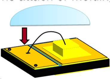
Color temperature of the LED dependins on thickness of the phosphor layer. When LED is complete the manufactures (assemblers) start their selections process called binning.
There are several parameters which are under strict selection procedures in companies: Luminous Intensity (rank), Forward Voltage, CCT (Correlated Color Temperature – practically, saying the LED it is in range of cool, natural or warm colour)
Strong players on the led market keep the total control of each part of the production process including housing/hosting/sourcing/keeping? wafer production in house, this example could be Seoul Semiconductor or Cree.
